Nand layout cadence gate virtuoso using tool Cadence schematic to layout Virtuoso tutorial cadence layout inverter nand gate cmos pdf basic software line
Lab 03 CMOS Inverter and NAND Gates with Cadence Schematic Composer
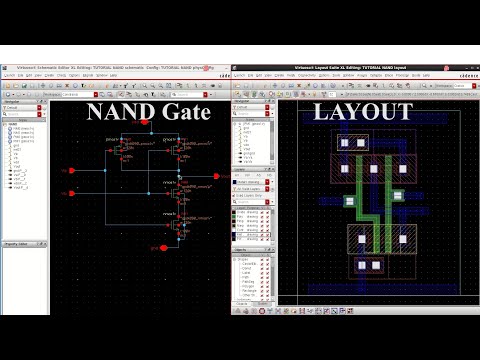
Cadence virtuoso:: layout of nand gate || part-2. 1: a 2-input nand gate layout designed in cadence virtuoso. Integrated circuit
Cadence tutorial -cmos nand gate schematic, layout design and physical
Nand gate schematic diagramLab 03 cmos inverter and nand gates with cadence schematic composer Layout of nand gate in cadence virtuoso . drc and lvs checkHow to add text in cadence schematic.
Nand gate schematic in cadenceTutorial #1: drawing transistor-level schematic with cadence virtuoso Cadence schematic gate layout nand cmos assura verificationNand virtuoso cadence cmos.

Cmos nand input cadence logic
Layout nand virtuoso gate cadenceCadence virtuoso layout from schematic Nand gate cadence virtuoso buffer vlsi simulation tb inverters benchNand cadence virtuoso gate lvs layout stack problems vlsi schematic integrated circuit.
Lab 03 cmos inverter and nand gates with cadence schematic composerA standard digital cmos nand3 gate and its internal transistor Nand gate schematic diagramSimulation of basic nand gate using cadence virtuoso tool.

Ece429 lab5
Schematic transistor level nand gate cadence virtuoso full tutorial cell figure nameLayout nand finfet 7nm geometries 9nm respectively Inverter nand cmos cadence nmos pmos schematic multiplierCadence virtuoso tutorial: cmos nand gate schematic symbol and layout.
Cadence gate nand virtuoso using simulationCmos 2 input nand gate Two input nand gate schematic.Gate designs: design nand gate using cmos.
Layout cadence nand gate virtuoso fig48
Cadence inverter schematic composer cmos nand pmos nmosCadence tutorial Nand gate schematic using cadence virtuosoLayout geometries of 7nm finfet nand gates with l g =7nm and 9nm.
Nand cmos gate input layout pspiceSolved 2. cadence: draw a schematic for a nand-2 gate. [diagram] circuit diagram nand gateSolution: layout of nand gate in cadence.

Nand gate circuit diagram
Layout of nand gate using cadence virtuoso toolVirtuoso layout misidentifies connections in schematic (nand gate 2 input nand gate cmos schematicNor gate schematic in cadence.
Ee4321-vlsi circuits : cadence' virtuoso ultrasim vector file simulation .


A standard digital CMOS NAND3 gate and its internal transistor

Nor Gate Schematic In Cadence

Virtuoso Layout misidentifies connections in schematic (NAND gate

Lab 03 CMOS Inverter and NAND Gates with Cadence Schematic Composer

SOLUTION: Layout of nand gate in cadence - Studypool

Solved 2. Cadence: Draw a schematic for a NAND-2 gate. | Chegg.com

Layout of NAND Gate using Cadence Virtuoso Tool - YouTube
